Rui Wang

Research

Ferroelectrics and dielectrics

Goal. Describe how charged point defects (oxygen vacancies, electrons, holes) move and react in oxide ferroelectrics and dielectrics, and how they change domain walls and electrical properties.

Significance. These defects screen domain walls, alter local conductivity, and drive the degradation and breakdown of capacitor dielectrics. The Ph.D. work developed a phase-field model that treats charged defects as mobile, reacting species coupled to polarization and the electric potential.

Charged domain walls in BiFeO₃in preparation

Head-to-head and tail-to-tail domain walls carry bound charge, which free carriers and oxygen vacancies move in to screen. The model resolves which species screen the wall, to what extent, and how the screening changes the wall width and conductivity. In the dissertation results, free charges screen the bound charge only partially, which is relevant to domain-wall electronics.
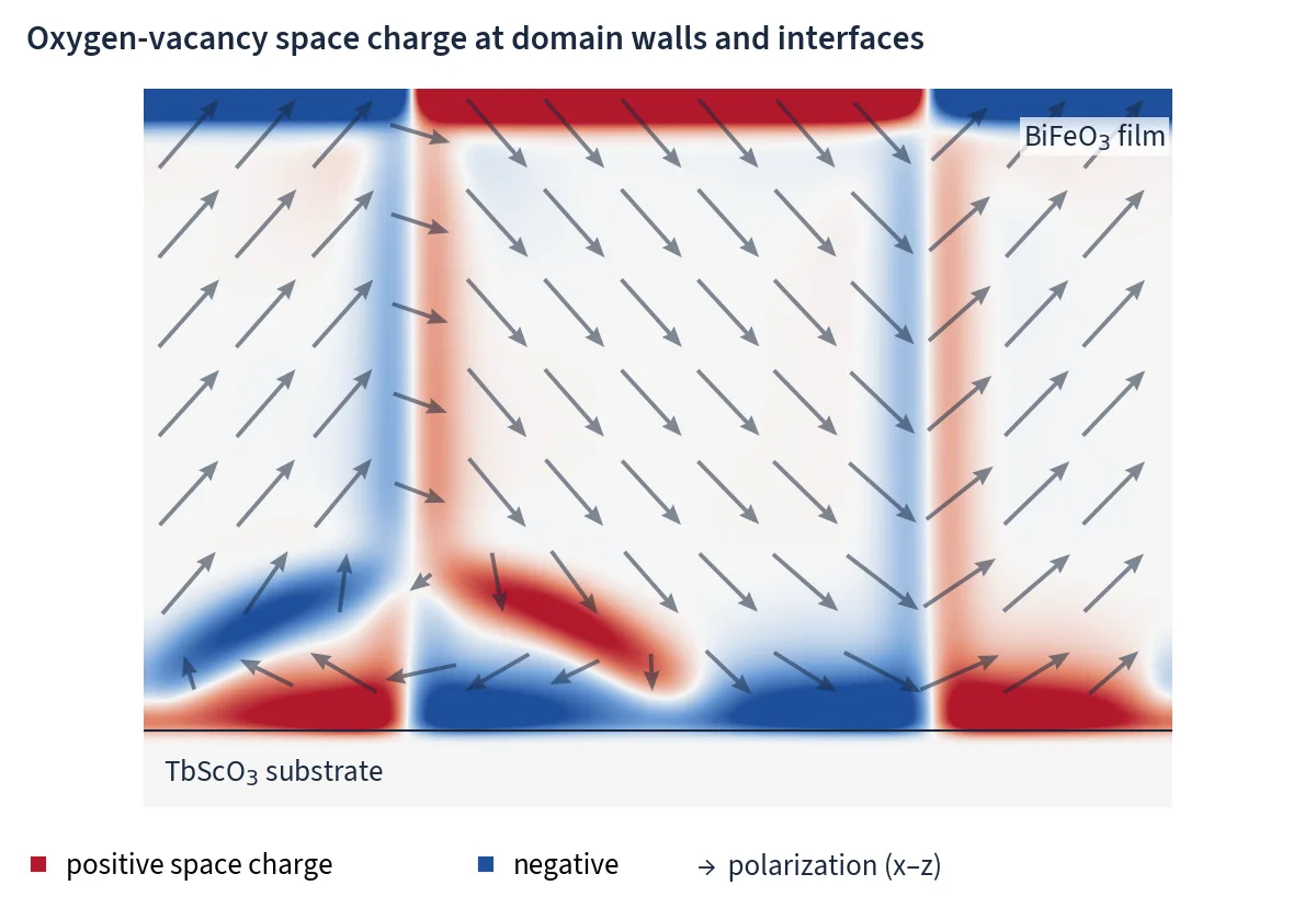
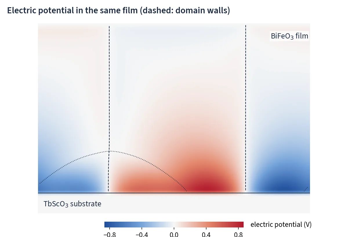
Cross-section of a BiFeO3 film on a TbScO3 substrate. Space charge (red = positive, blue = negative) builds up at the domain walls, along a wedge domain and at both interfaces, as oxygen vacancies redistribute.
Space-charge map with polarization arrows
Final state with polarization arrows: the free charge sits where the polarization changes direction.
Electric potential map
Electric potential in the same film; dashed lines mark the domain walls.
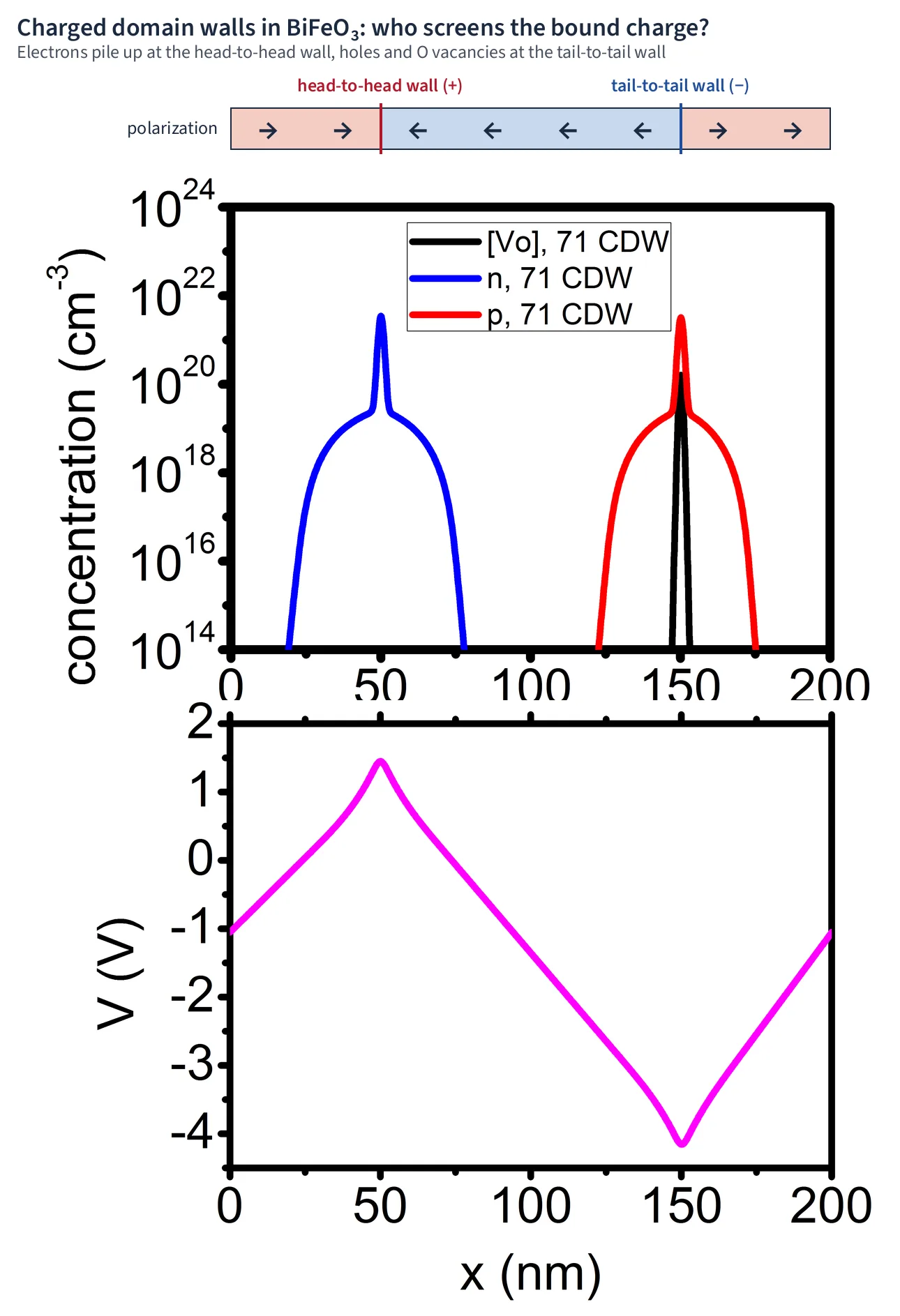
Concentration and potential profiles across charged walls
71° charged walls in bulk BiFeO3: electrons gather at the head-to-head wall, holes and vacancies at the tail-to-tail wall, with a potential swing of about 5 V between them.
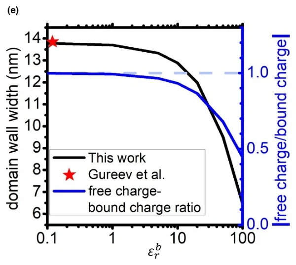
Domain wall width and free-to-bound charge ratio
Wall width and the ratio of free to bound charge versus the background dielectric constant. The free charge falls short of the bound charge, so the screening is incomplete. Star: analytical width of Gureev et al. From the dissertation, Fig. 3-4(e).

Papers: Ph.D. dissertation 2022
Model: R. Wang (Ph.D. research, L.-Q. Chen group, Penn State). The BiFeO3/TbScO3 film simulation is from a 2021 collaborative study. Journal papers in preparation.

Dielectric degradation and breakdownin preparation

Capacitor dielectrics gradually lose their insulation under field and temperature. The model describes this resistance degradation in Fe-doped SrTiO3 by coupling vacancy migration with charge injection from the electrodes, and it produces quantities that can be compared directly with experiments: leakage current over time, conductivity profiles and impedance spectra.

Own code In-house code: model and code developed by R. Wang; no commercial software.
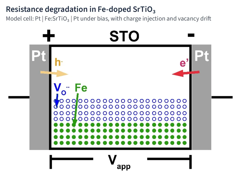
Schematic of the Pt / Fe:SrTiO3 / Pt model cell
Model cell: Fe-doped SrTiO3 between Pt electrodes under bias, with charge injection and vacancy drift.
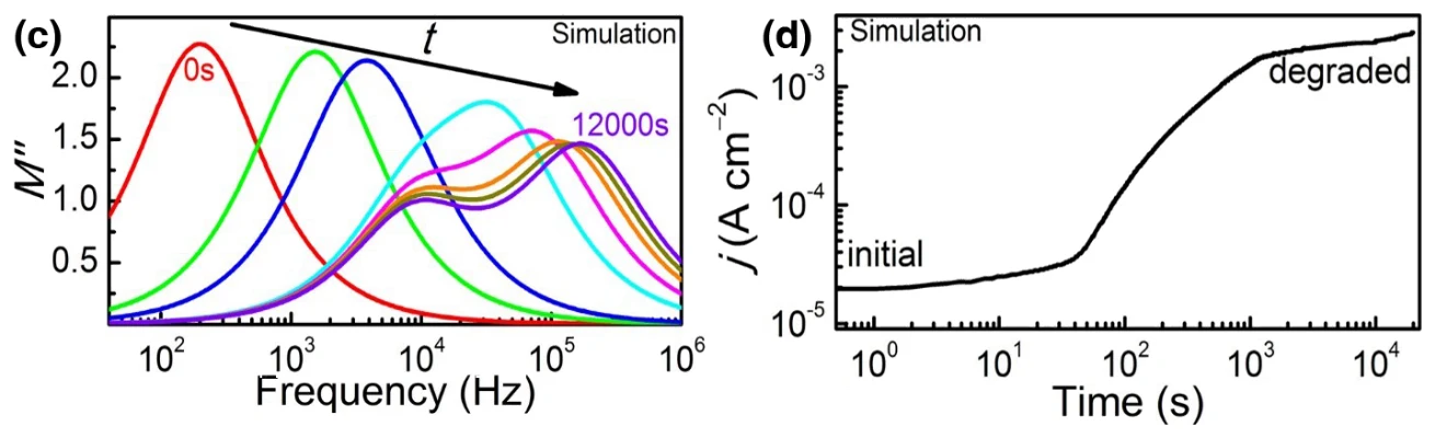
Simulated modulus spectra and leakage current during degradation
Simulated degradation of Fe-doped SrTiO3 (40 V across 0.5 mm, 210 °C). Left: the electric-modulus peak shifts and splits over 12,000 s. Right: the leakage current climbs by two orders of magnitude. Both match in-situ measurements. From the dissertation, Fig. 2-6(c, d).
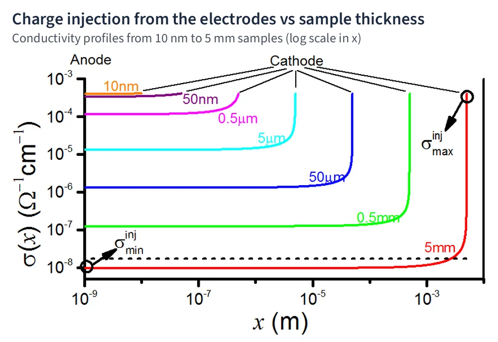
Conductivity profiles for different sample thicknesses
Charge injection from the electrodes dominates thin samples: conductivity profiles from 10 nm to 5 mm thick. Dissertation Fig. 2-5; Appl. Phys. Lett. 2017.

Papers: Ph.D. dissertation 2022 · Appl. Phys. Lett. 2017 · J. Am. Ceram. Soc. 2019
Model and code: R. Wang, with J.-J. Wang and L.-Q. Chen (Penn State), in collaboration with the C. A. Randall group. Journal paper in preparation.